
Description
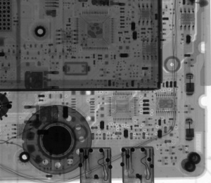
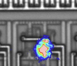
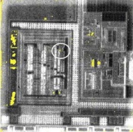
Photoemission Microscopy is a non-destructive imaging technique used to visualize electrical, chemical, and surface properties of semiconductor devices at high spatial resolution. By detecting electrons emitted from the sample surface under ultraviolet or X-ray illumination, this method reveals surface potential variations, work function differences, and contamination. Photoemission microscopy is valuable for identifying defects, performance-limiting features, and failure mechanisms in semiconductor devices.
Applications
- Surface Potential Mapping:Visualize variations in electrical potential across semiconductor surfaces.
- Defect Localization:Identify surface defects, contamination, or oxidation affecting device performance.
- Failure Analysis:Detect regions contributing to leakage, shorts, or degradation in ICs and microelectronic devices.
- Material Characterization:Assess work function, chemical states, and surface modifications.
- Reliability Testing:Monitor changes under electrical or thermal stress conditions.
- Quality Control:Ensure surface integrity and consistency in high-precision semiconductor components.
- Research & Development:Support device optimization, new material evaluation, and microelectronic process studies.


Reviews
There are no reviews yet.