

Description
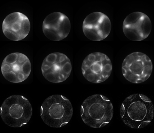
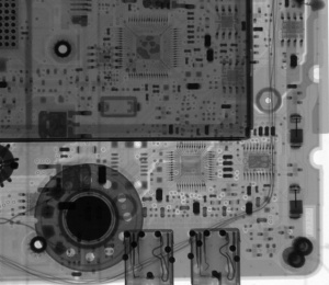
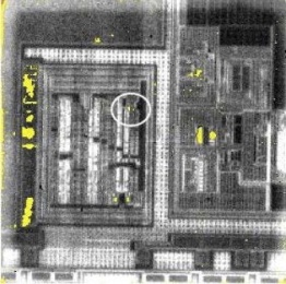
Thermal Emission Microscopy (also known as Thermal or Infrared Emission Imaging) is a non-destructive technique used to visualize localized heating and hot spots in semiconductor devices under electrical operation. By detecting infrared radiation emitted from the device, this method identifies regions with excessive current density, resistive heating, or defects that could lead to failure. Thermal emission microscopy is widely used for failure analysis, reliability testing, and design verification of ICs and microelectronic components.
Applications
- Hot Spot Detection:Identify localized overheating in transistors, ICs, and other semiconductor devices.
- Failure Analysis:Locate defective regions causing shorts, leakage, or excessive power dissipation.
- Design Verification:Evaluate thermal performance and current distribution in device layouts.
- Reliability Assessment:Monitor device behavior under operational stress and thermal cycling.
- Quality Control:Detect process variations or defects that may affect device performance.
- Research & Development:Support optimization of semiconductor design, materials, and packaging.
- Power Electronics & Microelectronics: Assess thermal management and performance of high-current or high-power components.
Reviews
There are no reviews yet.