Nanotechnology Singapore | Laboratory Equipment | Quasi-S
  • Home
  • Company
    • ABOUT US
  • Products
  • Services
    • LAB SERVICES
    • ENGINEERING SERVICES
  • Contact
    • INQUIRY
    • SAMPLES COLLECTION
Nanotechnology Singapore | Laboratory Equipment | Quasi-S
Menu
Click to enlarge
Home Lab Services Semiconductor Failure Analysis & Reliability Testing 2D & 3D X-Ray Analysis
Electrical Verification (I-V, Parametric Test)
Back to products
Photoemission Microscopy

2D & 3D X-Ray Analysis

Add to quote
This product is already in your quote request list.
Browse the list
  • Description
  • Reviews (0)
Description

Description

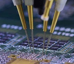
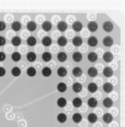
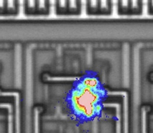
2D and 3D X-Ray Analysis is a non-destructive technique used to visualize the internal structures of semiconductor devices, PCBs, and electronic components. 2D X-ray provides flat images for quick inspection, while 3D X-ray (computed tomography) reconstructs the internal volume, allowing detailed visualization of solder joints, wire bonds, voids, and hidden defects. This method is essential for failure analysis, quality control, and reliability assessment without dismantling the device.

Applications

  • Internal Defect Detection:Identify voids, cracks, delamination, and solder joint issues in semiconductor packages and PCBs.
  • Wire Bond & Flip-Chip Inspection:Examine internal connections, bumps, and bond integrity.
  • Package Verification:Assess multilayer structures, encapsulation, and hidden features.
  • Failure Analysis:Locate defects contributing to electrical or mechanical failures.
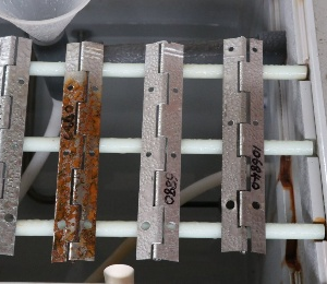
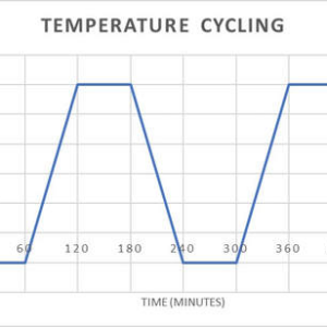
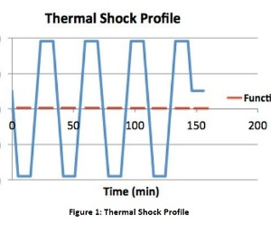
  • Reliability Assessment:Monitor defects and structural integrity over thermal or mechanical stress tests.
  • Quality Control:Verify soldering quality, component placement, and internal assembly consistency.
  • Research & Development:Support package design optimization, materials evaluation, and new device prototyping.
Reviews (0)

Reviews

There are no reviews yet.

Be the first to review “2D & 3D X-Ray Analysis” Cancel reply

Your email address will not be published. Required fields are marked *

Related Application

Confocal Scanning Acoustic Microscopy (CSAM)

Add to quote
This product is already in your quote request list.
Browse the list

High Temperature Oven Test

Add to quote
This product is already in your quote request list.
Browse the list

Optical Beam Induced Resistance Change (OBIRCH)

Add to quote
This product is already in your quote request list.
Browse the list

Photoemission Microscopy

Add to quote
This product is already in your quote request list.
Browse the list

Salt Spray Test

Add to quote
This product is already in your quote request list.
Browse the list

Solderability Test

Add to quote
This product is already in your quote request list.
Browse the list

Temperature & Humidity Cycling Test

Add to quote
This product is already in your quote request list.
Browse the list

Thermal Shock Test

Add to quote
This product is already in your quote request list.
Browse the list
    © Quasi-S Pte. Ltd. . All right reserved.

    company

    Products

    Services

    contact

    Quasi-S Pte Ltd
    (HQ)

    35 Marsiling Industrial Estate Road 3 #04-03, Singapore 739257.

    T (65) 6383 4386
    F (65) 6383 3071
    E contact@quasi-s.com.sg

    Quasi-S Sdn Bhd
    (Bangi Branch)

    Block Stroma B3-1, UKM-MTDC Smart Technology Centre 43600 Bangi, Selangor, Malaysia

    T (603) 8210 1765
    F (603) 8920 2506
    E inquirybangi@quasi-s.com.my

    Quasi-S Sdn Bhd
    (Penang Branch)

    15-G-26 Bayan Point Medan Kampung Relau 11900 Penang, Malaysia

    T (604) 645 6973
    F (60) 4645 6573
    E inquiry@quasi-s.com.my

    • Home
    • Company
      • ABOUT US
    • Products
    • Services
      • LAB SERVICES
      • ENGINEERING SERVICES
    • Contact
      • INQUIRY
      • SAMPLES COLLECTION