
Description
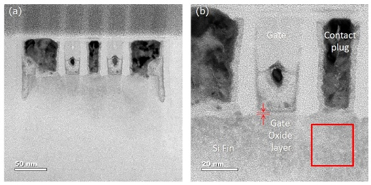
Transmission Electron Microscopy (TEM) is a high-resolution imaging technique that allows detailed visualization of the internal structure of materials at the nanometer and even atomic scale. By transmitting a beam of electrons through ultra-thin samples, TEM provides information on morphology, crystallography, defects, and composition that is beyond the capabilities of optical or scanning electron microscopes. TEM is widely used for research and quality control across a variety of industries, including semiconductors, materials science, nanotechnology, and biological sciences.
Applications
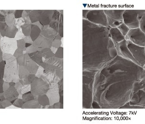
- Materials Characterization:Analyze microstructure, grain boundaries, and phase distribution in metals, ceramics, and polymers.
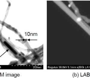
- Nanomaterials Analysis: Study nanoparticles, nanowires, nanotubes, and other nanostructures in detail.
- Defect and Failure Analysis:Detect dislocations, voids, inclusions, and other defects in industrial and electronic components.
- Crystallography and Lattice Imaging:Determine crystal structures, orientations, and atomic arrangements.
- Biological and Biomedical Research: Examine cell structures, viruses, and biomaterials at high resolution.
- Chemical Composition and Elemental Mapping:When combined with EDS (Energy Dispersive X-ray Spectroscopy), TEM provides elemental analysis and mapping at nanoscale.
- Thin Film and Coating Analysis:Characterize thickness, uniformity, and interface quality of coatings and thin films.
Reviews
There are no reviews yet.