Description
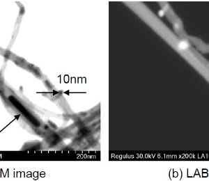
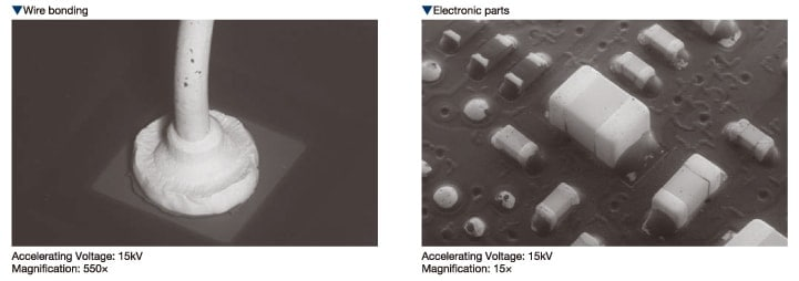
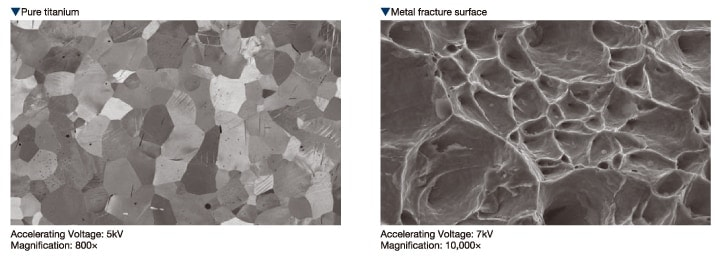
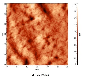
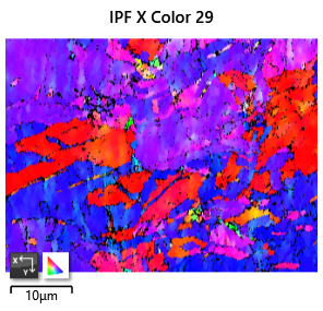
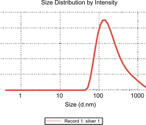
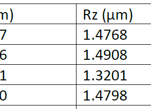
Scanning Electron Microscopy (SEM) is a high-resolution imaging technique that uses a focused electron beam to scan the surface of a sample. SEM provides detailed images of surface topography, microstructures, and morphology with magnifications far beyond conventional optical microscopy. It is widely used in metallurgical analysis, materials science, failure analysis, and research to study metals, alloys, polymers, ceramics, and coatings.
- Surface Topography: Examine fine surface features, roughness, and morphology at micro- to nanoscale.
- Microstructural Analysis: Observe grains, phases, precipitates, inclusions, and defects in metals and alloys.
- Fractography: Investigate fracture surfaces to determine failure mechanisms.
- Coatings & Thin Films: Analyze surface layers, uniformity, and defects.
- Failure Analysis: Identify cracks, voids, corrosion, and other material defects.
- Materials Research: Support development and characterization of metals, polymers, ceramics, and composites.


Reviews
There are no reviews yet.