
Description
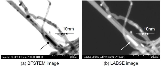
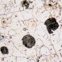
Scanning Transmission Electron Microscopy (STEM) is an advanced electron microscopy technique that combines features of SEM and TEM. A finely focused electron beam scans a thin sample, transmitting electrons through it to produce high-resolution images of internal structures. STEM allows atomic-scale imaging, crystallography, and compositional analysis, making it essential for nanomaterials, semiconductors, and advanced metallurgical research.
Applications
- Nanostructure Analysis: Visualize atomic arrangements, grain boundaries, and defects at the nanoscale.
- Thin Film & Coating Examination:Measure thickness, uniformity, and internal morphology.
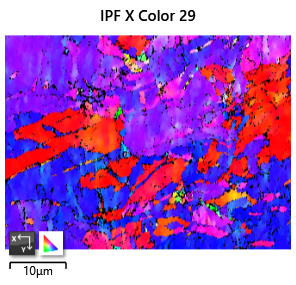
- Crystallography & Phase Identification:Analyze crystal structures, orientation, and defects.
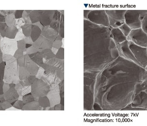
- Failure Analysis: Investigate nanoscale defects causing device or material failure.
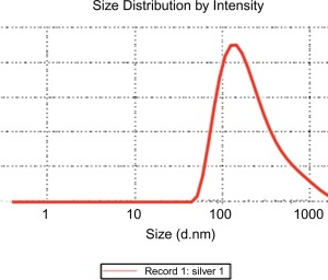
- Elemental & Compositional Mapping: Perform high-resolution mapping using EDS or EELS.
- Materials Research: Characterize advanced alloys, nanomaterials, ceramics, and semiconductor

Reviews
There are no reviews yet.