Nanotechnology Singapore | Laboratory Equipment | Quasi-S
  • Company
  • Products
  • Services
  • Contact
Nanotechnology Singapore | Laboratory Equipment | Quasi-S
Menu
SIGRAY AttoMap-310 Micro-XRF with high resolution and sensitivity
Click to enlarge
Home Synchrotron Lab-Based System Micro - XRF SIGRAY AttoMap-310 Micro-XRF
QATM Qness 250/750/3000E EVO Macro Hardness Tester - A versatile hardness tester supporting Brinell, Knoop, Rockwell, and Vickers methods.
QATM Qness 250/750/3000E EVO Macro Hardness Tester
Back to products
CAFRAMO Model BDC2002 Compact Digital Stirrer with Stirlight™ feature for clear solution visibility
CAFRAMO Model BDC2002 Compact Digital Stirrer

SIGRAY AttoMap-310 Micro-XRF

The Sigray AttoMap™ is a powerful X-ray fluorescence microscope with the highest resolution and highest sensitivity laboratory fluorescence capabilities available, enabled by patented technology. The AttoMap-310 has advance exclusive features in addition to features that are also in the AttoMap-200.

Add to quote
This product is already in your quote request list.
Browse the list
  • Description
Description

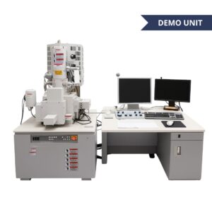
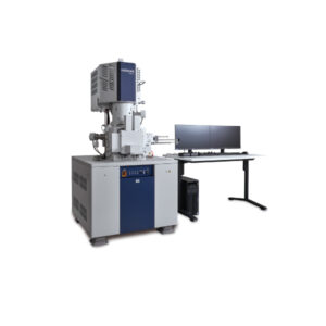
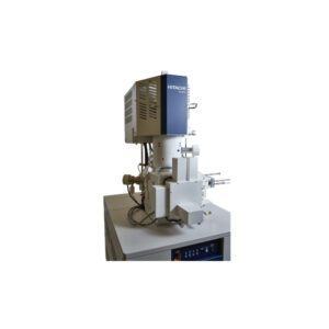
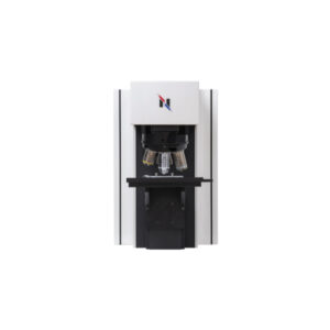
The SIGRAY AttoMap-310 Micro-XRF is a groundbreaking X-ray fluorescence microscope that sets new standards in laboratory fluorescence capabilities. Certainly, with its highest resolution and sensitivity, the AttoMap-310 achieves down to single-digit microns (3-5 µm) and sub-ppm sensitivity, making it an indispensable tool for detailed elemental analysis. Furthermore, this advanced system features energy tunability with up to five different incident X-ray spectra, allowing for optimized imaging across a broad range of samples. Additionally, the AttoMap-310’s large travel and enclosure enable unsupervised overnight scans, providing opportunities to integrate correlative techniques such as Raman Spectroscopy. Whether for life sciences, environmental studies, mineralogy, or semiconductor research, the SIGRAY AttoMap-310 Micro-XRF offers unparalleled performance and versatility.

Features SIGRAY AttoMap-310 Micro-XRF

Highest resolution laboratory microXRF

Achieve down to single digit microns (3-5µm) with high resolution optic

Sub-ppm sensitivity

Quantify down to sub parts per million (ppm) levels with Sigray’s flexible software packages

Energy tunability

Maximize throughout and sensitivity with up to 5 different incident X-ray spectra

Large Travel and Enclosure

Enables unsupervised overnight scans. Also provides opportunity to integrate correlative techniques such as Raman Spectroscopy

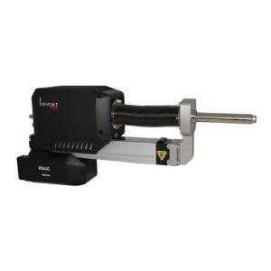
Patented Multi-Target Ultrahigh Brightness X-ray Source

Sigray’s X-ray source, when combined with the X-ray opticas, has over 50X the brightness over the illumination beam (source+optics) systems employed by other leading microXRF systems. Up to 4 target materials can be customized for the AttoMap-200 source, allowing software selection optimal spectra for your sample

Achieves shallow angle imaging for thin samples (e.g., biological) and/or diffraction removal

AttoMap-310 features a goniometer to enable normal to shallow angle of incidence imaging

Light element detection

Analyse down to trace-level organics within the AttoMap’s high vacuum chamber

Energy Tunability for High Throughput and Sensitivities

Comparison-source-targets-1

Comparison of As channel in a arsenopyrite sample. Arsenic sensitivity is dramatically increased because of the substantially better As fluorescence cross-section for Mo than W.

Energy Tunability for High Throughput and Sensitivities

Source-target-materials

Select up to 5 elements for your AttoMap-310 X-ray source. Examples are given above but additional targets (e.g., Ti, Ag, etc.) may be provided upon request.

Application of SIGRAY AttoMap-310 Micro-XRF

  • Life Sciences and Metallomics
  • Environmental / Botany
  • Mineralogy
  • Semiconductor
  • Light Element Detection

Elemental Channels of a Daphnia Water Flea
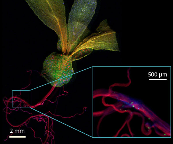
Hyperaccumulating

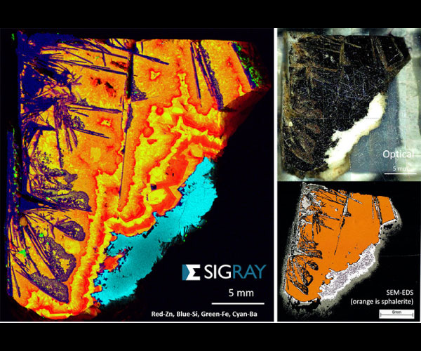
Mineralogical mapping using Sigray’s AttoMap (left), a correlative optical image acquired with the AttoMap (upper right), and a SEM-EDS image of the same sample.

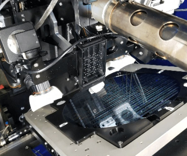
300mm wafer in AttoMap

    AttoMap-310 provides detection of elements down to B and enables trace-level (<1%) quantification of organics such as C, O, N. This is accomplished through the system’s incorporation of a specialized low energy detector and a vacuum enclosure that achieves evacuated environments of better than 10^-4 Torr. The system can also be run in ambient mode for maximum flexibility.

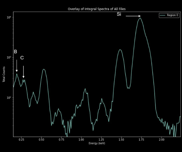
    Low Z element detection including Boron

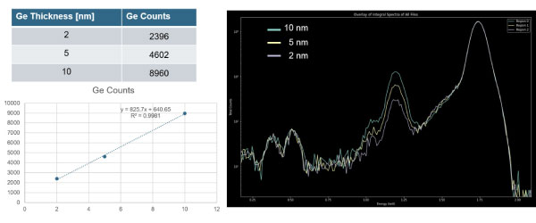
    Linearity of Ge (2nm, 5nm, and 10nm) in a silicon wafer

      Related Application

      Bruker QUANTAX EDS Flash 7 Detector for Advanced Elemental Analysis

      BRUKER QUANTAX EDS (Energy-Dispersive X-Ray Spectroscopy)

      Add to quote
      This product is already in your quote request list.
      Browse the list
      Oxford Ultim® Max EDS Detector for Advanced EDS Analysis

      OXFORD Ultim® Max EDS Detector

      Add to quote
      This product is already in your quote request list.
      Browse the list
      OXFORD Xplore EDS Detector for SEM Analysis

      OXFORD Xplore EDS Detector

      Add to quote
      This product is already in your quote request list.
      Browse the list
      SIGRAY QuantumLeap-V210 X-ray Absorption Spectroscopy (XAS) system

      SIGRAY QuantumLeap-V210

      Add to quote
      This product is already in your quote request list.
      Browse the list
      Hitachi SU3800 SEM Demo Unit showcasing advanced imaging capabilities
      Hitachi SU3800 SEM Demo Unit showcasing advanced imaging capabilities

      HITACHI SU3800 SEM (Demo Unit)

      Add to quote
      This product is already in your quote request list.
      Browse the list
      Hitachi SU8600 Ultra-High-Resolution Scanning Electron Microscope (SEM)

      HITACHI SU8600 Ultrahigh-Resolution SEM

      Add to quote
      This product is already in your quote request list.
      Browse the list
      Bruker-Nanophoton Random Scanning Confocal Raman Microscopy RamanWalk for precise and efficient Raman imaging
      ruker-Nanophoton Random Scanning Confocal Raman Microscopy RamanWalk for precise and efficient Raman imaging

      BRUKER-NANOPHOTON Random Scanning Confocal Raman Microscopy RamanWalk

      Add to quote
      This product is already in your quote request list.
      Browse the list

      EVACTRON TEM WAND™ System

      Add to quote
      This product is already in your quote request list.
      Browse the list
        © Quasi-S Pte. Ltd. . All right reserved.

        company

        Products

        Services

        contact

        Quasi-S Pte Ltd
        (HQ)

        35 Marsiling Industrial Estate Road 3 #04-03, Singapore 739257.

        T (65) 6383 4386
        F (65) 6383 3071
        E contact@quasi-s.com.sg

        Quasi-S Technology Sdn Bhd
        (Bangi Branch)

        Block Stroma B3-1, UKM-MTDC Smart Technology Centre 43600 Bangi, Selangor, Malaysia

        T (603) 8210 1765
        F (603) 8920 2506
        E inquirybangi@quasi-s.com.my

        Quasi-S Sdn Bhd
        (Penang Branch)

        15-G-26 Bayan Point Medan Kampung Relau 11900 Penang, Malaysia

        T (604) 645 6973
        F (60) 4645 6573
        E inquiry@quasi-s.com.my

        • Company
        • Products
        • Services
        • Contact