
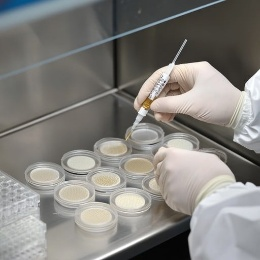
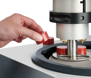
Description
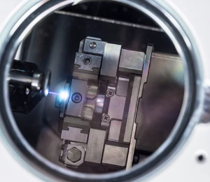
Sputter Coating is a sample preparation technique used to deposit a thin conductive layer, typically of gold, platinum, or carbon, onto non-conductive or low-conductivity samples. This process improves imaging quality in electron microscopy by reducing charging effects and enhancing signal resolution. Sputter coating is widely applied for SEM analysis of biological samples, polymers, ceramics, and electronic components.
Applications
- Biological Samples:Enhance imaging of cells, tissues, and microorganisms by preventing charging.
- Polymers & Ceramics:Improve SEM imaging of insulating materials.
- Electronics & PCBs:Prepare non-conductive components for high-resolution surface inspection.
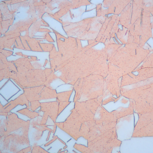
- Nanomaterials & Microstructures:Enable clear imaging of nanoparticles, fibers, and micro/nano features.
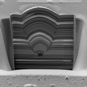
- Failure Analysis:Support observation of cracks, delamination, and other structural defects.
- Surface Characterization:Enhance contrast and detail in morphology studies.
- Research & Development:Prepare samples for high-resolution imaging in materials science, life sciences, and engineering applications.
Reviews
There are no reviews yet.