
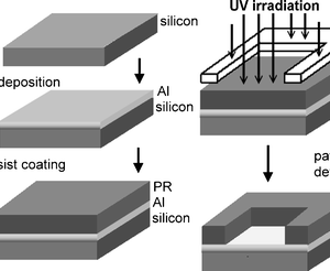
Description
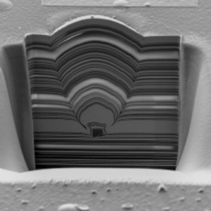
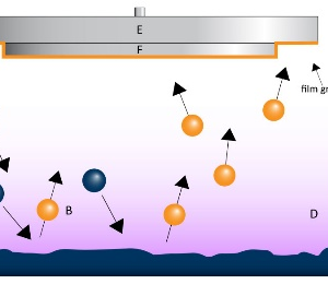
Ion Milling is a precise sample preparation technique that uses a focused ion beam to remove material from a sample, creating flat, polished, or cross-sectional surfaces with minimal mechanical damage. This non-contact method preserves delicate features, sharp interfaces, and microstructures, making it ideal for high-resolution imaging in SEM, and microanalysis. The system is capable of flat milling, cross-section milling, and site-specific preparation for advanced materials and electronic components.
Applications
- Cross-Section Preparation:Create high-quality cross-sections of metals, semiconductors, ceramics, and composites.
- Flat Surface Polishing:Produce artifact-free, smooth surfaces for imaging and analysis.
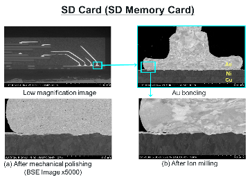
- Microelectronics & PCBs:Reveal internal structures, solder joints, and multilayer features.
- Nanomaterials & Thin Films:Prepare delicate nanostructures without altering morphology or composition.
- Failure & Defect Analysis:Investigate cracks, delamination, voids, and layer interfaces.
- Advanced Materials Research:Support site-specific sample preparation for SEM, and microanalysis.
- Quality Control:Ensure consistent sample preparation for inspection of coatings, devices, and composite materials.

Reviews
There are no reviews yet.