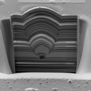
The Sigray XADA (X‑ray Assisted Device Alteration) system is a groundbreaking solution for semiconductor circuit debugging and fault isolation, especially for modern architectures such as Backside Power Delivery (BPD). Traditional debugging methods like Laser Assisted Device Alteration (LADA) struggle with new designs that shift power delivery to the device’s backside. In contrast, XADA uses focused X‑rays that penetrate intact devices with little to no sample thinning, enabling rapid and effective fault identification.
Because XADA employs a highly focused, high‑flux X‑ray beam, it achieves micron‑scale probing that can reveal time delays and performance variations at small scales. This capability allows engineers to quickly isolate critical signal paths (“speedpaths”) and understand failure mechanisms in high‑performance chips used in automotive, mobile, and AI processing applications. Moreover, using X‑rays eliminates the preparation steps required by optical or laser techniques, reducing turnaround time and enabling more direct analysis of devices under test.
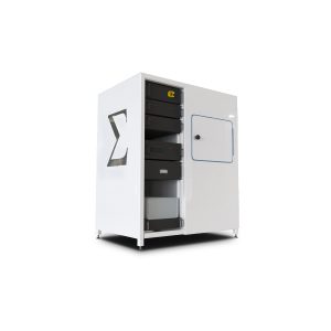
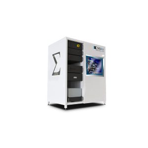
The system is designed from the ground up to accommodate a wide variety of test setups. With a large and flexible tester area, XADA enables efficient positioning of diverse tester designs. Its layout also minimizes expensive cable handling by allowing movement of testers into and out of the system without disconnecting cabling, saving setup time and reducing wear on test hardware.
Key Features of Sigray XADA 200
X‑ray Based Device Alteration
- Replaces older laser‐based techniques with X‑ray probing to reach backside features without complex sample preparation.
Micron‑Scale Resolution
- Achieves focused X‑ray beam spot sizes down to single digits in microns, supporting detailed circuit debug.
High‑Flux X‑ray Probing
- Provides intense X‑ray exposure to induce measurable circuit time shifts for rapid identification of critical paths.
Flexible Tester Integration
- Designed with ample tester space and long cable runs, enabling seamless integration with existing test systems.
Patent‑Pending Optics and Source
- Uses advanced X‑ray optics and patented source technologies for reliable, high‑performance operation.
Applications of Sigray XADA 200
The XADA system is especially effective in semiconductor research and manufacturing environments that require advanced fault isolation and performance analysis. Typical applications include:
-
Backside Power Delivery (BPD) circuit debug in advanced chips
-
Failure analysis and speedpath isolation in microelectronic devices
-
Performance characterization of high‑speed logic and analog circuits
-
Advanced metrology workflows in semiconductor R&D and quality labs
By combining X‑ray penetration power with focused microprobe capability, Sigray XADA empowers engineers to uncover intricate device behaviors and accelerate development cycles. Its flexible design supports evolving technologies, enabling labs to tackle next‑generation semiconductor challenges with confidence.

First-of-its-kind X-ray Assisted Device Alteration
XADA uses a highly focused, high-intensity X-ray beam to induce measurable time delays in circuits, enabling fast identification of critical signal paths, or “speedpaths.” Unlike traditional LADA systems, XADA is specifically designed for modern backside power delivery (BPD) architectures, where power lines are moved to the backside of the device. Its penetrating X-rays allow circuit debugging with minimal or no sample preparation, making it an essential solution for next-generation high-performance chips used in automotive, mobile, and AI applications.

Microns-Scale X-ray Probing
XADA’s small probe size is enabled by patented and patent-pending innovations in x-ray source and x-ray optics technologies.
Sigray is the world leader in x-ray optics and has developed advanced fabrication capabilities under several large government grants over the past decade. The company now supplies its x-ray focusing optics to most synchrotron facilities. Due to its heavy R&D investment in x-ray optics, Sigray is the only company in the world capable of fabricating double-paraboloidal x-ray optics with the stringent straightness and surface profile tolerance requirements needed for XADA. Optics used for XADA are produced through a patent-pending process that maximizes symmetry and minimizes slope errors. Additional patent-pending innovations in x-ray source and optics are expected to enable Sigray XADA probes to achieve submicron spot sizes in the future.
Using X-rays, 3-4 ps shifts in circuit delays can be seen.

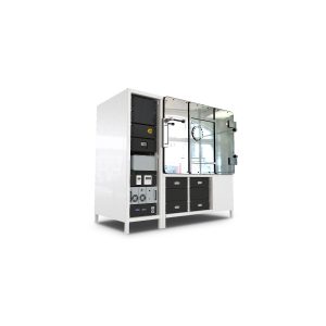
Configured and Designed for Testers
Sigray collaborated with industrial thought leaders to develop a system with a large, flexible tester area to accommodate a wide variety of tester designs. To reduce costs associated with expensive tester cables, the system was also designed with large cable runs, minimizing cable lengths and allowing testers to be moved into and out of the XADA unit without disconnecting the cables.