")

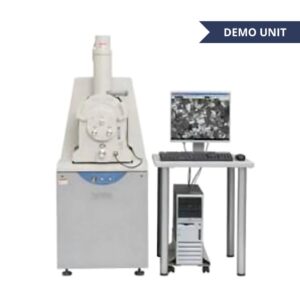
The HITACHI S-4800 FE-SEM is a high-resolution cold field emission SEM designed for advanced surface and materials characterization at the nanoscale. With exceptional imaging capabilities down to 1.0 nm at 15 kV, it provides sharp, detailed images of microstructures with outstanding depth of field.
Equipped with the Horiba EMAX Evolution EDX system, this setup enables precise elemental analysis and compositional mapping, making it ideal for both imaging and microanalysis in a wide range of applications.
Key Features of HITACHI S-4800 FE-SEM:
- Resolution: 1.0 nm (15 kV, WD = 4mm)
1.4 nm (1 kV, WD = 1.5mm, Deceleration mode*1)
2nm (1kV, WD = 1.5mm, Normal mode)
- Accelerating voltage: 0.5 to 30 kV (Normal mode)
(Landing voltage) 0.1 to 2.0kV (Deceleration mode*1)
- Cold field emission source for high beam stability and brightness
- Dual secondary electron detectors (upper and lower)
- Integrated Horiba EMAX Evolution EDX system for qualitative and semi-quantitative elemental analysis
- Large chamber suitable for various sample types
| Type I | |
| Stage Control | Manual, 3-axis motor drive (X,Y,R)* |
| Movable Range
X Y Z T R |
0 – 50mm* 0 – 50mm* 1.5 – 30mm – 5 to +70° 360°* |
| Sample size (maximum) | 100mm dia. (standard) |
*3-axis motor drive
Movable range is limited to the size of the mounted specimen.
Electrical Image Shift : ± 12um (WD = 8mm)
Detectors: Secondary electron detector (Upper/Lower)
Electron dispersive x-ray detector (EDS)
Applications of HITACHI S-4800 FE-SEM:
- Nanomaterials and surface morphology analysis
- Failure analysis (FA) in semiconductors and electronics
- Elemental identification and mapping in PCBA and thin films
- Materials science, metallurgy, and life sciences (non-biological samples)
The Hitachi S-4800 with Horiba EMAX Evolution EDX offers a powerful combination of imaging and analysis, trusted by researchers and engineers in R&D labs, academic institutions, and high-tech industries.