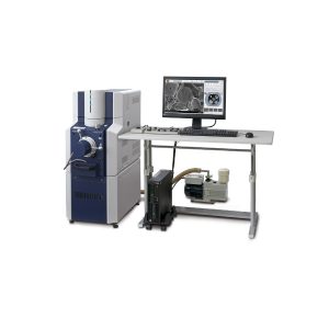
Features:
- High-resolution STEM imaging
– HAADF-STEM image 0.136 nm, FFT image 0.105 nm (optional HR lens)
– BF STEM image 0.204 nm (w/o Cs-corrector) - High-speed & high-sensitivity EDX analysis: Probe current × 10 times
– Timely and rapid elemental mapping
– Low-concentration element detection - Hitachi-developed Cs-corrector
– Equipped with a probe-forming spherical aberration corrector developed by Hitachi, the automatic aberration-correction process takes a short time and does not require prior experience for aberration correction - Seamless solution from sample preparation to observation & analysis
– Holder compatible with Hitachi Focused Ion Beam (FIB)
Application
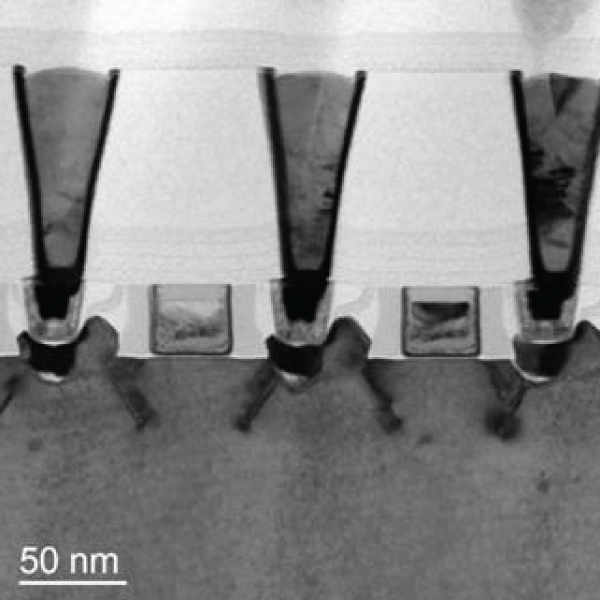
Cross Section BF-STEM Images of 32 nm NMOS Transistor
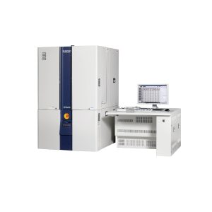
HD-2700 with aberration corrector
Acceleration Voltage : 200 kV